Two-dimensional materials have attracted considerable research interest because their properties can differ markedly from those of their bulk counterparts, opening up possibilities for new electronic and spintronic technologies. Among them, two-dimensional magnetic materials are particularly intriguing, although controlling their magnetic behavior at room temperature remains a major challenge.
Can the dielectric layer beneath a two-dimensional magnet help influence its magnetic properties? Yiting Mo and colleagues investigated this question using Fe₃GeTe₂ nanosheets on silicon-based substrates. By varying the thickness of the SiOₓ dielectric layer and comparing measurements in darkness and under ultraviolet illumination, they explored how the substrate interface relates to the material’s room-temperature magnetic response.
This question is especially relevant for Fe₃GeTe₂, a layered metallic magnet whose bulk magnetic transition temperature lies below room temperature. To investigate the influence of the substrate, the researchers studied surface-oxidized nanosheets on Si/SiOₓ structures with dielectric thicknesses of 50, 100, 200 and 300 nm. Measurements under 365 nm ultraviolet illumination provided a further way to examine changes in the nanosheets’ magnetic and electronic responses.
Understanding these changes required more than measuring the magnetic response alone. AFM topography established the nanosheet morphology and helped identify corresponding measurement regions. Using NANOSENSORS PPP-LC-MFMR AFM probes with a low-coercivity, soft magnetic coating, magnetic force microscopy (MFM) mapped magnetic force-related phase contrast. Kelvin probe force microscopy (KPFM), performed with NANOSENSORS PPP-EFM AFM probes with a conductive Pt/Ir coating, measured contact-potential differences. Together, these techniques allowed the researchers to examine how local magnetic and electronic measurements varied with dielectric thickness and illumination.
The measurements revealed a pronounced dependence on the underlying oxide layer. On 50 nm SiOₓ, the Fe₃GeTe₂ nanosheets exhibited substantial MFM phase contrast at room temperature. This contrast decreased under UV illumination and recovered when the illumination was removed, while KPFM measurements also showed a change in contact-potential difference between dark and illuminated conditions.
The response was markedly different on the thickest dielectric layer. At 300 nm SiOₓ, the MFM phase signal was much weaker, approaching the reported measurement noise level, and the illumination-dependent response was minimal. Results from the intermediate thicknesses supported the broader trend of decreasing magnetic contrast and optical response with increasing dielectric thickness. The accompanying KPFM observations revealed related changes in contact potential, providing complementary information about the electronic response.
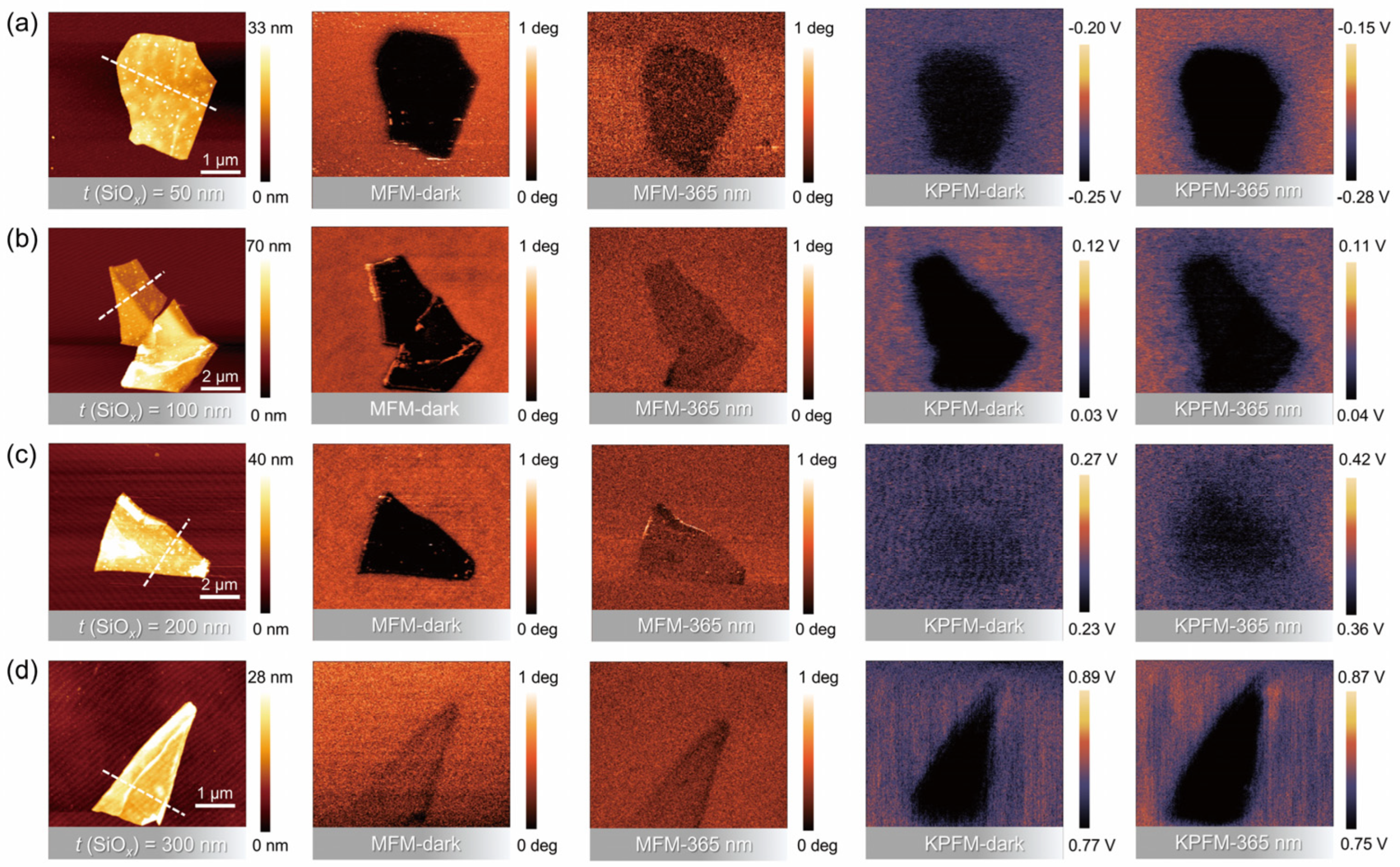
AFM, MFM and KPFM measurements of Fe₃GeTe₂ nanosheets on Si/SiOₓ substrates. Rows (a–d) show SiOₓ thicknesses of 50, 100, 200 and 300 nm, respectively. Each row combines AFM topography with magnetic force microscopy (MFM) and Kelvin probe force microscopy (KPFM) images under dark conditions and 365 nm UV illumination. The study used NANOSENSORS PPP-LC-MFMR probes for MFM and PPP-EFM probes for KPFM. Complete original Figure 2 from Mo et al., Nanomaterials 16, 596 (2026), https://doi.org/10.3390/nano16100596. Reproduced under CC BY 4.0.
Because MFM measures magnetic force-related contrast rather than magnetic ordering directly, the researchers also examined the material using complementary techniques. In particular, room-temperature polar magneto-optical Kerr effect (MOKE) measurements showed magnetic hysteresis loops for both the 50 nm and 300 nm dielectric conditions. These observations provide additional evidence for magnetic ordering and help place the local MFM results in context: weak MFM contrast at the larger dielectric thickness does not necessarily mean that magnetism is absent.
The combined observations also raise the question of what produces the thickness-dependent behavior. The authors attribute these trends to interfacial charge transfer and dielectric screening. They propose that interfacial charges have a stronger influence on the magnetic response when the SiOₓ layer is thin, whereas thicker dielectric layers increasingly screen this influence. The accompanying changes in KPFM potential and MFM phase contrast support this interpretation without independently establishing the underlying microscopic mechanism.
The findings highlight the importance of the dielectric interface in understanding room-temperature magnetic responses in Fe₃GeTe₂ nanosheets. By combining nanoscale magnetic and electronic measurements with complementary magnetic characterization, the study provides a basis for investigating how substrate design and illumination may help tune two-dimensional magnetic systems.
Featured Publication
Yiting Mo, Yijun Huang, Haotian Xu, Shijing Wang, Liang Hu and Lingwei Li.
Room Temperature Ferromagnetism Engineered in Two-Dimensional Metallic Magnets via Metal–Insulator–Semiconductor Structures.
Nanomaterials 16, 596 (2026).
https://doi.org/10.3390/nano16100596
Open access under Creative Commons Attribution (CC BY 4.0).
Image Attribution and License
Complete original Figure 2 from Mo et al., Nanomaterials 16, 596 (2026), https://doi.org/10.3390/nano16100596. Reproduced under Creative Commons Attribution 4.0 International (CC BY 4.0): https://creativecommons.org/licenses/by/4.0/.
The separate Featured Image is an adapted layout of Figure 2(a), showing only the 50 nm SiOₓ condition. Its five original measurement panels have been rearranged for presentation.