Insights into dynamic sliding contacts from conductive atomic force microscopy
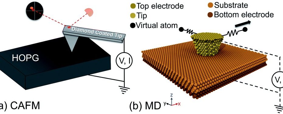
Friction in nanoscale contacts is determined by the size and structure of the interface that is hidden between the contacting bodies. One approach to investigating… Read More »Insights into dynamic sliding contacts from conductive atomic force microscopy


