Electrostatic Force Microscopy (EFM) is an important atomic force microscopy (AFM) technique for investigating electrical properties and electrostatic interactions at the nanoscale. Achieving quantitative EFM measurements requires a precise understanding of the contact potential difference (VCPD) between the AFM probe and the sample surface. In this article, Lukas Lehnert, Ronald Thoelen, and Hildegard Möbius investigate the influence of AFM probe geometry on contact potential difference measurements and propose an improved model for interpreting Electrostatic Force Microscopy data.
The authors combine experimental measurements with theoretical analysis to examine the individual contributions of the AFM probe apex and cantilever cone to electrostatic interactions. While conventional EFM models generally assume an equipotential AFM probe and treat the contact potential difference as an additional applied voltage, the study demonstrates that this simplified approach cannot fully explain experimentally observed voltage parabolas. By separating the electrostatic contributions of the probe apex and cantilever cone, the proposed model provides a more accurate description of tip–sample interactions during EFM measurements.
Atomic force microscopy experiments were performed in lift mode to maximize the signal-to-noise ratio while minimizing topographic contributions. The study compared two AFM probe designs, including the NANOSENSORS SSS-MFMR AFM probe and an uncoated silicon reference probe, enabling direct evaluation of how AFM probe geometry, magnetic coating, and tip characteristics influence quantitative electrostatic measurements. To eliminate variations arising from manufacturing tolerances, the same individual AFM probe was used throughout each measurement series.
The NANOSENSORS SSS-MFMR AFM probe features a cobalt chromium-coated silicon tip with a nominal tip radius of approximately 15 nm, a spring constant of 2.8 N/m, and a resonance frequency of 75 kHz. Rather than relying on nominal tip dimensions, the authors determined the effective AFM probe radius for every individual experiment to compensate for probe wear and deformation, significantly improving the quantitative accuracy of Electrostatic Force Microscopy measurements.
This work demonstrates how careful AFM probe characterization, combined with improved electrostatic modeling, advances the quantitative interpretation of Electrostatic Force Microscopy and Kelvin Probe Force Microscopy experiments. The findings highlight the importance of selecting an appropriate NANOSENSORS AFM probe for high-precision EFM and KPFM investigations and contribute to a deeper understanding of nanoscale tip–sample electrostatic interactions.
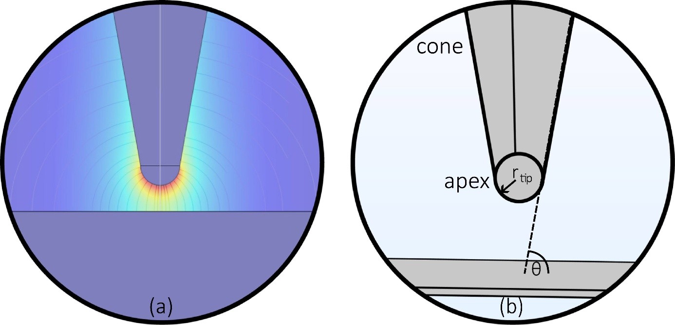
Figure 1. Equivalent models for the tip-substrate interaction: (a) Simulation: solving Poisson’s equation for conducting tip and substrate(red = high and blue = low electric field strength) [23]; (b) analytical model by Hudlet [17, 18]: contribution of cantilever, cone and apex of the tip (exact tip form needed).
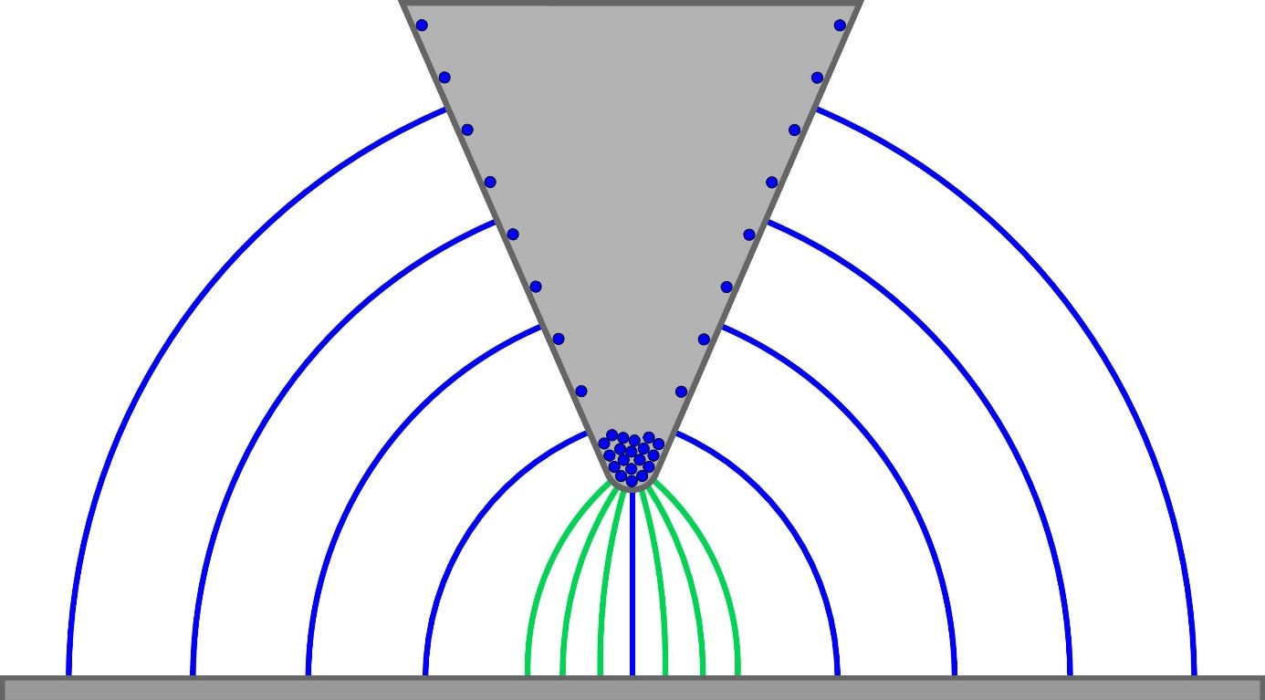
Figure 2. Schematic illustration of charge concentration at the apex of the AFM probe due to VDC, leading to a reduction of the interaction area. In contrast, VCPD leads to a increased interaction area due to the charge distribution on the cone surface to maintain VCPD.
Full citation:
Lehnert, L.; Thoelen, R.; Möbius, H.
Revisiting Contact Potential Difference in Electrostatic Force Microscopy.
Journal of Physics Communications 10 (2026), 015007.
https://doi.org/10.1088/2399-6528/ae381f
Creative Commons license: CC BY 4.0