Graphene is one of the most extensively studied 2D materials, exhibiting extraordinary mechanical and electronic properties. *
Although many years have passed since its discovery, manipulating single graphene layers is still challenging using standard resist-based lithography techniques. *
Recently, it has been shown that it is possible to etch graphene directly in water-assisted processes using the so-called focused electron-beam-induced etching (FEBIE), with a spatial resolution of ten nanometers. *
Nanopatterning graphene with such a method in one single step and without using a physical mask or resist is a very appealing approach. *
In the article “Graphene removal by water-assisted focused electron-beam-induced etching – unveiling the dose and dwell time impact on the etch profile and topographical changes in SiO2 substrates “ Aleksandra Szkudlarek, Jan M. Michalik, Inés Serrano-Esparza, Zdeněk Nováček, Veronika Novotná, Piotr Ozga, Czesław Kapusta and José María De Teresa describe how, during the process, on top of graphene nanopatterning, they found significant morphological changes induced in the SiO2 substrate even at low electron dose values (<8 nC/μm2). *
They demonstrate that graphene etching and topographical changes in SiO2 substrates can be controlled via electron beam parameters such as dwell time and dose. *
The feasibility of water-assisted FEBIE, available on scanning electron microscopes operating in low-vacuum mode, makes the method very promising for prototyping various optical/electronic devices based on graphene. *
In their article, Aleksandra Szkudlarek et al. show that with certain precautions water-assisted FEBIE can be applied for such a nanopatterning process. *
The experimental data obtained with scanning Raman spectroscopy, correlative probe and electron microscopy, and in situ AFM measurements provide a comprehensive image of FEBIE etch profiles. *
Additionally, the etching process is accompanied by morphological changes in the microstructure of the substrate – likely occurring during exposure to the ambient air and pressure. Complementary studies performed using both in situ and ex situ AFM reveal the modification in SiO2/Si substrate topography. *
Precise surface analysis of etched structures can be performed by atomic force microscopy. The authors used an AFM setup capable of integrating into a scanning electron microscope (SEM). They used the correlative probe and electron microscopy (CPEM) technology for simultaneous acquisition of AFM and SEM signals, enabling an efficient and complex surface analysis.
The AFM-in-SEM approach allowed for in situ analysis.
Thus, the graphene could be modified and immediately measured by AFM without changing the environment. *
The analysis was performed by using the tapping mode and the NANOSENSORS™ Akiyama probe (a tuning fork based self-sensing and self-actuating AFM probe, A-Probe).*
Data shown in Figure 4 of the cited article (also shown here in the blogpost) were measured with the following parameters: scan speed of 20 µm/m, scan range of 20 µm × 20 µm, and image resolution of 512 × 512 pixels. The resonance frequency of the particular AFM probe was 43 kHz. *

Figure 4 from Aleksandra Szkudlarek et al 2024 “Graphene removal by water-assisted focused electron-beam-induced etching – unveiling the dose and dwell time impact on the etch profile and topographical changes in SiO2 substrates” :
Results of in situ AFM measurements of the etched lines on the SiO2/Si substrate as a function of the dwell time: A) AFM profiles of lines etched with different dwell times (td = 1, 10, and100 μs); B) 3D AFM image of the SiO2 surface.
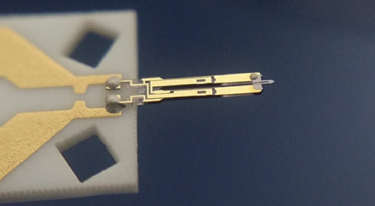
NANOSENSORS self-sensing and self-actuating Akiyama-probe
*Aleksandra Szkudlarek, Jan M. Michalik, Inés Serrano-Esparza, Zdeněk Nováček, Veronika Novotná, Piotr Ozga, Czesław Kapusta and José María De Teresa
Graphene removal by water-assisted focused electron-beam-induced etching – unveiling the dose and dwell time impact on the etch profile and topographical changes in SiO2 substrates
Beilstein Journal of Nanotechnology 2024, 15, 190–198
DOI: https://doi.org/10.3762/bjnano.15.18
Open Access: The article “Graphene removal by water-assisted focused electron-beam-induced etching – unveiling the dose and dwell time impact on the etch profile and topographical changes in SiO2 substrates” by Aleksandra Szkudlarek, Jan M. Michalik, Inés Serrano-Esparza, Zdeněk Nováček, Veronika Novotná, Piotr Ozga, Czesław Kapusta and José María De Teresa is licensed under a Creative Commons Attribution 4.0 International License, which permits use, sharing, adaptation, distribution and reproduction in any medium or format, as long as you give appropriate credit to the original author(s) and the source, provide a link to the Creative Commons license, and indicate if changes were made. The images or other third party material in this article are included in the article’s Creative Commons licence, unless indicated otherwise in a credit line to the material. If material is not included in the article’s Creative Commons licence and your intended use is not permitted by statutory regulation or exceeds the permitted use, you will need to obtain permission directly from the copyright holder. To view a copy of this licence, visit https://creativecommons.org/licenses/by/4.0/.