NANOSENSORS PPP-NCSTAu probes were used for scanning probe characterizations for this publication.
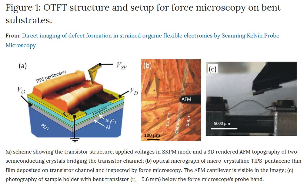
Figure 1: OTFT structure and setup for force microscopy on bent substrates. From: T. Cramer et. al., Direct imaging of defect formation in strained organic flexible electronics by Scanning Kelvin Probe Microscopy
For the full article have a look at:
https://www.nature.com/articles/srep38203
![]() The article “Direct imaging of Defect Formation in Strained Organic Flexible Electronics by Scanning Kelvin Probe Microscopy” by Tobias Cramer et. al. is licensed under a Creative Commons Attribution 4.0 International License. To view a copy of this license, visit http://creativecommons.org/licenses/by/4.0/
The article “Direct imaging of Defect Formation in Strained Organic Flexible Electronics by Scanning Kelvin Probe Microscopy” by Tobias Cramer et. al. is licensed under a Creative Commons Attribution 4.0 International License. To view a copy of this license, visit http://creativecommons.org/licenses/by/4.0/