Okumura B, Yamaguchi E, Komura N, Ohtomi T, Kawano SI, Sato H, Katagiri H, Ando H, Ikeda M
Photodegradable glyco-microfibers fabricated by the self-assembly of cellobiose derivatives bearing nitrobenzyl groups
Communications Materials. 2024 Sep 10;5(1):182
DOI: https://doi.org/10.1038/s43246-024-00622-0
Vivanco-Chávez P, Klichowicz M, Popov O, Lieberwirth H, Heide G, Mertens F
Atomic Force Microscopy as a Means to Analyze Vickers Indentation Experiments: Crack Morphology, Fracture Toughness, and Indentation Profile
Minerals (2075-163X). 2024 Dec 1;14(12)
DOI: https://doi.org/10.3390/min14121193
Shintani Y, Katagiri H, Ikeda M
Oxidation‐responsive supramolecular hydrogel based on a simple fmoc‐cysteine derivative capable of showing autonomous gel–sol–gel transitions
Advanced Functional Materials. 2024 Jun;34(25):2312999
DOI: https://doi.org/10.1002/adfm.202312999
Liu H, Vampa G, Zhang JL, Shi Y, Buddhiraju S, Fan S, Vuckovic J, Bucksbaum PH, Reis DA
Beating absorption in solid-state high harmonics
Communications Physics. 2020 Oct 30;3(1):192
DOI: https://doi.org/10.1038/s42005-020-00472-5
Rognin E, Landis S, Davoust L
Viscoelastic leveling of annealed thin polystyrene films
Langmuir. 2014 Jun 17;30(23):6963-9
DOI: https://doi.org/10.1021/la5009279
Lorenzoni M, Giugni A, Torre B
Oxidative and carbonaceous patterning of Si surface in an organic media by scanning probe lithography
Nanoscale research letters. 2013 Feb 13;8(1):75
DOI: https://doi.org/10.1186/1556-276X-8-75
Torre B, Basso M, Tiribilli B, Paoletti P, Vassalli M
Disclosing and overcoming the trade-off between noise and scanning speed in atomic force microscopy
Nanotechnology. 2013 Jul 18;24(32):325104
DOI: https://doi.org/10.1088/0957-4484/24/32/325104
Juang BJ, Huang KY, Liao HS, Leong KC, Hwang S
AFM pickup head with holographic optical element (HOE)
In2010 IEEE/ASME International Conference on Advanced Intelligent Mechatronics 2010 Jul 6 (pp. 442-446). IEEE
DOI: https://doi.org/10.1109/AIM.2010.5695758
Jo A, Joo W, Jin WH, Nam H, Kim JK
Ultrahigh-density phase-change data storage without the use of heating
Nature Nanotechnology. 2009 Nov;4(11):727-31
DOI: https://doi.org/10.1038/nnano.2009.260
Hwu ET, Hung SK, Yang CW, Huang KY, Hwang S
Real-time detection of linear and angular displacements with a modified DVD opticalhead
Nanotechnology. 2008 Feb 18;19(11):115501
DOI: https://doi.org/10.1088/0957-4484/19/11/115501
Ikeda M, Ueno S, Matsumoto S, Shimizu Y, Komatsu H, Kusumoto KI, Hamachi I
Three‐Dimensional Encapsulation of Live Cells by Using a Hybrid Matrix of Nanoparticles in a Supramolecular Hydrogel
Chemistry–A European Journal. 2008 Nov 26;14(34):10808-15
DOI: https://doi.org/10.1002/chem.200801144
Kwon SJ, Jeong YM, Jeong SH
Fabrication of high-aspect-ratio silicon nanostructures using near-field scanning optical lithography and silicon anisotropic wet-etching process Applied Physics A. 2007 Jan;86(1):11-8
DOI:
https://doi.org/10.1007/s00339-006-3744-4


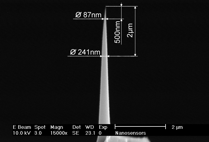
 Due to their unique geometry the tips of the are more susceptible to tip damage by electrostatic discharge (ESD) than other Silicon-SPM-Probes.