ATEC-NCAu

Cantilever data:
Property Nominal Value Specified Range
Resonance Frequency [kHz] 335 210 - 490
Force Constant [N/m] 45 12 - 110
Length [µm] 160 150 - 170
Mean Width [µm] 45 40 - 50
Thickness [µm] 4.6 3.6 - 5.6
Order codes and shipping units:
Order Code AFM probes per pack
ATEC-NCAu-10 10

Special handling information for NANOSENSORS™ AdvancedTEC probes

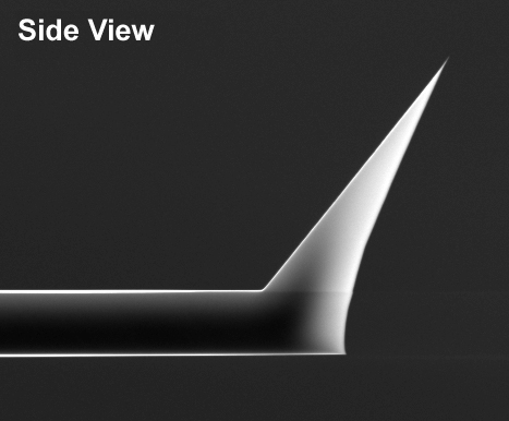
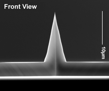
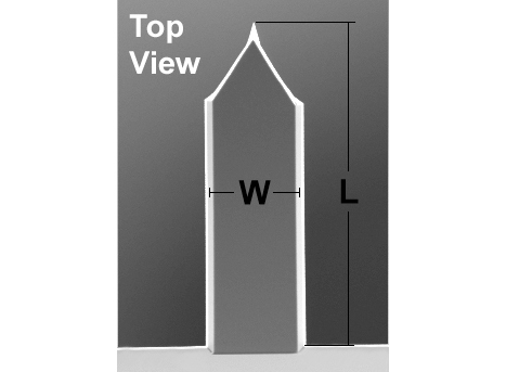
Due to their unique geometry the tips of the AdvancedTEC probes are more susceptible to tip damage by electrostatic discharge (ESD) than other Silicon-SPM-Probes.

Electric fields near the probe chip may lead to field evaporation which can blunt the tip apex of the probe tip. Therefore the NANOSENSORS™ AdvancedTEC probes are shipped in specially designed ESD-safe chip carriers.

NANOSENSORS™ recommends to their customers to take appropriate precautions to avoid tip damage due to electrostatic discharge when handling the probes. This can for example be done by using anti-electrostatic mats, wrist bands and tweezers.

NANOSENSORS™ AdvancedTEC™ AFM Probes

Advanced Tip at the End of the Cantilever™Non-Contact/Tapping Mode, Au coated

NANOSENSORS™ AdvancedTEC™ NCAu AFM tips are designed for non-contact or tapping mode imaging. They feature a tetrahedral AFM tip that protrudes from the very end of the AFM cantilever. This unique feature allows precise positioning and makes the AdvancedTEC™ the only AFM scanning probe in the world that offers REAL TIP VISIBILITY FROM TOP, even when the AFM probe is tilted due to its mounting onto the AFM head. This feature makes them the premium choice for all applications where the AFM tip has to be placed exactly on the point of interest and/or has to be visible (e.g. Nanomanipulation).

Due to their very small half cone angles the AFM tips of the AdvancedTEC™ Series show great performance on samples that have a small pattern size combined with steep sample features.

The AFM probe offers unique features:

  • real AFM tip visibility from top
  • metallic conductivity of the AFM tip
  • AFM tip height 15 - 20 µm
  • high mechanical Q-factor for high sensitivity

The metallic coating is an approximately 70 nm thick double layer of chromium and gold on both sides of the AFM cantilever.The tip side coating enhances the conductivity of the AFM tip and allows electrical contacts. The detector side coating enhances the reflectivity of the laser beam by a factor of about 2 and prevents light from interfering within the AFM cantilever. The coating process is optimized for stress compensation and wear resistance. As the coating is nearly stress-free the bending of the AFM cantilever due to stress is less than 2 degrees.

Please note: Wear at the AFM tip can occur if operating in contact-, friction- or force modulation mode or where it is necessary to conduct high currents.

Zhang T, Chen S, Petkov PS, Zhang P, Qi H, Nguyen NN, Zhang W, Yoon J, Li P, Brumme T, Alfonsov A
Two-dimensional polyaniline crystal with metallic out-of-plane conductivity
Nature. 2025 Feb 5:1-7
DOI: https://doi.org/10.1038/s41586-024-08387-9


Romashkina A, Sushil S, Barreda AI, Fedorova Z, Abtahi F, Doolaard N, Zhang Z, Helgert C, Staude I, Eilenberger F, Pertsch T
Enhanced Exciton–Plasmon Interaction Enabling Observation of Near-Field Photoluminescence in a WSe2–Gold Nanoparticle Hybrid System
ACS Photonics. 2025 May 5.
DOI: https://doi.org/10.1021/acsphotonics.4c01989


Yamamoto T, Yamane H, Yokoshi N, Oka H, Ishihara H, Sugawara Y
Optical imaging of a single molecule with subnanometer resolution by photoinduced force microscopy
ACS nano. 2023 Dec 29;18(2):1724-32
DOI: https://doi.org/10.1021/acsnano.3c10924


Kisiel M, Brovko OO, Yildiz D, Pawlak R, Gysin U, Tosatti E, Meyer E
Mechanical dissipation from charge and spin transitions in oxygen-deficient SrTiO3 surfaces
Nature communications. 2018 Jul 27;9(1):2946
DOI: https://doi.org/10.1038/s41467-018-05392-1