Dmitry Khalenkow, Alejandro Diaz Tormo, Anne De Meyst, Louis Van Der Meeren, Joost Verduijn, Joanna Rybarczyk, Daisy Vanrompay, Nicolas Le Thomas and Andre G Skirtach
Chlamydia psittaci infected cell studies by 4Pi Raman and atomic force microscopy
Microscopy, Volume 73, Issue 4, August 2024, Pages 335–342
DOI: https://doi.org/10.1093/jmicro/dfae011
Ning Li , Li Zhang , Ou Qiao , Xinyue Wang , Linyan Xu and Yanhua Gong
Special contribution of atomic force microscopy in cell death research
Nanotechnology Reviews (2024), Volume 13 Issue 1, pp. 20230208
DOI: https://doi.org/10.1515/ntrev-2023-0208
Alexina Ollier, Marcin Kisiel, Xiaobo Lu, Urs Gysin, Martino Poggio, Dmitri K. Efetov and Ernst Meyer
Energy dissipation on magic angle twisted bilayer graphene
nature Communications Physics volume 6, Article number: 344 (2023)
DOI: https://doi.org/10.1038/s42005-023-01441-4
Kohei Ono, Ayumi Iwata, Takeshi Fukuma, Yoko Iwamoto, Koji Hamasaki and Atsushi Matsuki
Characterization of adhesivity of organic enriched sea spray aerosols by atomic force microscopy
Atmospheric Environment, Volume 294, 1 February 2023, 119468
DOI: https://doi.org/10.1016/j.atmosenv.2022.119468
Ayana Yamagishi, Mei Mizusawa, Koki Uchida, Masumi Iijima, Shun’ichi Kuroda, Kyoko Fukazawa, Kazuhiko Ishihara and Chikashi Nakamura
Mechanical detection of interactions between proteins related to intermediate filament and transcriptional regulation in living cells
Biosensors and Bioelectronics, Volume 216, 15 November 2022, 114603
DOI: https://doi.org/10.1016/j.bios.2022.114603
Iuliia Efimova, Elena Catanzaro, Louis Van der Meeren, Victoria D Turubanova, Hamida Hammad, Tatiana A Mishchenko, Maria V Vedunova, Carmela Fimognari, Claus Bachert, Frauke Coppieters, Steve Lefever, Andre G Skirtach, Olga Krysko and Dmitri V Krysko
Vaccination with early ferroptotic cancer cells induces efficient antitumor immunity
Journal for Immunotherapy of Cancer. 2020; 8(2): e001369.
DOI: 10.1136/jitc-2020-001369
Thales F. D. Fernandes, Oscar Saavedra-Villanueva, Emmanuel Margeat, Pierre-Emmanuel Milhiet and Luca Costa
Synchronous, Crosstalk-free Correlative AFM and Confocal Microscopies/Spectroscopies
Nature Scientific Reports volume 10, Article number: 7098 (2020)
DOI: https://doi.org/10.1038/s41598-020-62529-3
Kohei Ono, Yuki Mizushima, Masaki Furuya, Ryota Kunihisa, Nozomu Tsuchiya, Takeshi Fukuma, Ayumi Iwata and Atsushi Matsuki
Direct Measurement of Adhesion Force of Individual Aerosol Particles by Atomic Force Microscopy
Atmosphere 2020, 11, 489
DOI: https://www.mdpi.com/2073-4433/11/5/489
Ayana Yamagishi, Moe Susaki, Yuta Takano, Mei Mizusawa, Mari Mishima, Masumi Iijima, Shun'ichi Kuroda, Tomoko Okada and Chikashi Nakamura
The Structural Function of Nestin in Cell Body Softening is Correlated with Cancer Cell Metastasis
International Journal of Biological Sciences 2019; 15(7): 1546–1556
DOI: 10.7150/ijbs.33423
Sergei Vlassov, Magnus Mets, Boris Polyakov, Jianjun Bian, Leonid Dorogin and Vahur Zadin
Abrupt elastic-to-plastic transition in pentagonal nanowires under bending
Beilstein Journal of Nanotechnology 2019, 10, 2468–2476
DOI: https://doi.org/10.3762/bjnano.10.237
Katharina Huttenlochner, Neda Davoudi, Christin Schlegel, Martin Bohley, Christine Müller-Renno, Jan C. Aurich, Roland Ulber and Christiane Ziegler
Paracoccus seriniphilus adhered on surfaces: Resistance of a seawater bacterium against shear forces under the influence of roughness, surface energy, and zeta potential of the surfaces
Biointerphases 13, 051003 (2018)
DOI: https://doi.org/10.1116/1.5049226
Yeoheung Yoon, Anand P. Tiwari, Minhe Lee, Min Choi, Wooseok Song, Jino Im, Taehyoung Zyung, Ha-Kyun Jung, Sun Sook Lee, Seokwoo Jeon and Ki-Seok An
Enhanced electrocatalytic activity by chemical nitridation of two-dimensional titanium carbide MXene for hydrogen evolution
Journal of Materials Chemistry A, 2018,6, 20869-20877
DOI: https://doi.org/10.1039/C8TA08197B
Danish Hussain, Yongbing Wen, Hao Zhang, Jianmin Song, and Hui Xie
Atomic Force Microscopy Sidewall Imaging with a Quartz Tuning Fork Force Sensor
Sensors 2018, 18(1), 100
DOI: https://doi.org/10.3390/s18010100
Marcin Kisiel, Oleg O. Brovko, Dilek Yildiz, Rémy Pawlak, Urs Gysin, Erio Tosatti and Ernst Meyer
Mechanical dissipation from charge and spin transitions in oxygen-deficient SrTiO3 surfaces
Nature Communications volume 9, Article number: 2946 (2018)
DOI: https://doi.org/10.1038/s41467-018-05392-1
Sergei Vlassov, Boris Polyakov, Mikk Vahtrus, Magnus Mets, Mikk Antsov, Sven Oras, Aivar Tarre, Tõnis Arroval, Rünno Lõhmus and Jaan Aarik
Enhanced flexibility and electron-beam-controlled shape recovery in alumina-coated Au and Ag core–shell nanowires
Nanotechnology (2017), Volume 28, 505707
DOI: 10.1088/1361-6528/aa973c
Akira Nagasaki, Saku T. Kijima, Tenji Yumoto, Miku Imaizumi, Ayana Yamagishi, Hyonchol Kim, Chikashi Nakamura and Taro Q.P. Uyeda
The Position of the GFP Tag on Actin Affects the Filament Formation in Mammalian Cells
Cell Structure and Function, 2017 Volume 42 Issue 2 Pages 131-140
DOI: https://doi.org/10.1247/csf.17016
Seunghwan Ryu, Yuta Matsumoto, Takahiro Matsumoto, Takafumi Ueno, Yaron R. Silberberg and Chikashi Nakamura
Improved efficiency of nanoneedle insertion by modification with a cell-puncturing protein
Japanese Journal of Applied Physics (2017) 57 03EB02
DOI: 10.7567/JJAP.57.03EB02
R. Kawamura, K. Shimizu, Y. Matsumoto, A. Yamagishi, Y. R. Silberberg, M. Iijima, S. Kuroda, K. Fukazawa, K. Ishihara and C. Nakamura
High efficiency penetration of antibody-immobilized nanoneedle thorough plasma membrane for in situ detection of cytoskeletal proteins in living cells
Journal of Nanobiotechnology volume 14, Article number: 74 (2016)
DOI: https://doi.org/10.1186/s12951-016-0226-5
Mikk Vahtrus, Andris Šutka, Boris Polyakov, Sven Oras, Mikk Antsov, Nicola Doebelin, Rünno Lõhmus, Ergo Nõmmiste and Sergei Vlassov
Effect of cobalt doping on the mechanical properties of ZnO nanowires
Materials Characterization, Volume 121, November 2016, Pages 40-47
DOI: https://doi.org/10.1016/j.matchar.2016.09.027
Sung-Woong Han, Hoon-Kyu Shin and Taiji Adachi
Nanolithography of Amyloid Precursor Protein Cleavage with β-Secretase by Atomic Force Microscopy
Journal of Biomedical Nanotechnology, Volume 12, Number 3, March 2016, pp. 546-553(8)
DOI: https://doi.org/10.1166/jbn.2016.2191
S. A. Meynell, A. Spitzig, B. Edwards, M. D. Robertson, D. Kalliecharan, L. Kreplak, and T. L. Monchesky
Structure of MnSi on SiC(0001)
Physical Review B (2016), 94, 184416
DOI: https://doi.org/10.1103/PhysRevB.94.184416
Mikk Vahtrus, Andris Šutka, Sergei Vlassov, Anna Šutka, Boris Polyakov, Rando Saar, Leonid Dorogin, Rünno Lõhmus
Mechanical characterization of TiO2 nanofibers produced by different electrospinning techniques
Materials Characterization, Volume 100, February 2015, Pages 98-103
DOI: https://doi.org/10.1016/j.matchar.2014.12.019
M. Kisiel, F. Pellegrini, G. E. Santoro, M. Samadashvili, R. Pawlak, A. Benassi, U. Gysin, R. Buzio, A. Gerbi, E. Meyer and E. Tosatti
Noncontact Atomic Force Microscope Dissipation Reveals a Central Peak of SrTiO3 Structural Phase Transition
Physical Review Letters (2015) 115, 046101
DOI: https://doi.org/10.1103/PhysRevLett.115.046101
Sergei Vlassov, Boris Polyakov, Leonid M. Dorogin, Mikk Vahtrus, Magnus Mets, Mikk Antsov,
Rando Saar, Alexey E. Romanov, Ants Lõhmus and Rünno Lõhmus
Shape Restoration Effect in Ag−SiO 2 Core−Shell Nanowires
Nano Letters 2014, 14, 5201−5205
DOI: https://doi.org/10.1021/nl5019063
Boris Polyakov, Sergei Vlassov, Leonid M. Dorogin, Jelena Butikova, Mikk Antsov, Sven Oras, Rünno Lõhmus and Ilmar Kink
Manipulation of nanoparticles of different shapes inside a scanning electron microscope
Beilstein Journal of Nanotechnology 2014, 5, 133–140
DOI: https://doi.org/10.3762/bjnano.5.13
Boris Polyakov, Mikk Antsov, Sergei Vlassov, Leonid M Dorogin, Mikk Vahtrus, Roberts Zabels, Sven Lange and Rünno Lõhmus
Mechanical properties of sol–gel derived SiO2 nanotubes
Beilstein Journal of Nanotechnology 2014, 5, 1808–1814
DOI: https://doi.org/10.3762/bjnano.5.191
Boris Polyakov, Sergei Vlassov, Leonid M Dorogin, Natalia Novoselska, Jelena Butikova, Mikk Antsov, Sven Oras, Runno Lohmus and Ilmar Kink
Some aspects of formation and tribological properties of silver nanodumbbells
Nanoscale Research Letters volume 9, Article number: 186 (2014)
DOI: https://doi.org/10.1186/1556-276X-9-186
Markus Langer, Marcin Kisiel, Rémy Pawlak, Franco Pellegrini, Giuseppe E. Santoro, Renato Buzio, Andrea Gerbi, Geetha Balakrishnan, Alexis Baratoff, Erio Tosatti and Ernst Meyer
Giant frictional dissipation peaks and charge-density-wave slips at the NbSe2 surface
Nature Materials volume 13, pages 173–177 (2014)
DOI: https://doi.org/10.1038/nmat3836
Leonid M. Dorogin, Sergei Vlassov, Boris Polyakov, Mikk Antsov, Rünno Lõhmus, Ilmar Kink, Alexey E. Romanov
Real-time manipulation of ZnO nanowires on a flat surface employed for tribological measurements: Experimental methods and modelling
IPPS, Volume 250, Issue 2, February 2013, Pages 305-317
DOI: https://doi.org/10.1002/pssb.201248445
Seunghwan Ryu, Ryuzo Kawamura, Ryohei Naka, Yaron R. Silberberg, Noriyuki Nakamura and Chikashi Nakamura
Nanoneedle insertion into the cell nucleus does not induce double-strand breaks in chromosomal DNA
Journal of Bioscience and Bioengineering, Volume 116, Issue 3, September 2013, Pages 391-396
DOI: https://doi.org/10.1016/j.jbiosc.2013.03.022
Yaron R. Silberberg, Shingo Mieda, Yosuke Amemiya, Toshiya Sato, Takanori Kihara, Noriyuki Nakamura, Kyoko Fukazawa, Kazuhiko Ishihara, Jun Miyake and Chikashi Nakamura
Evaluation of the actin cytoskeleton state using an antibody-functionalized nanoneedle and an AFM
Biosensors and Bioelectronics, Volume 40, Issue 1, 15 February 2013, Pages 3-9
DOI: https://doi.org/10.1016/j.bios.2012.06.044
Tomasz Bieniek, Grzegorz Janczyk, Paweł Janus, Piotr Grabiec, Marek Nieprzecki, Grzegorz Wielgoszewski, Magdalena Moczała, Teodor Gotszalk, Elizabeth Buitrago, Montserrat Fernandez-Bolaños Badia and Adrian M. Ionescu
Silicon nanowires reliability and robustness investigation using AFM-based techniques
SPIE Proceedings Volume 8902, Electron Technology Conference 2013; 89022L (2013)
DOI: https://doi.org/10.1117/12.2031229
Takahiro Watanabe-Nakayama, Masakazu Saito, Shin'ichi Machida, Kikuo Kishimoto, Rehana Afrin and Atsushi Ikai
Requirement of LIM domains for the transient accumulation of paxillin at damaged stress fibres
Biology Open (2013) 2 (7): 667–674
DOI: https://doi.org/10.1242/bio.20134531
Ryuji Hiramatsu, Toshiki Matsuoka, Chiharu Kimura-Yoshida, Sung-Woong Han, Kyoko Mochida, Taiji Adachi, Shuichi Takayama and Isao Matsuo
External Mechanical Cues Trigger the Establishment of the Anterior-Posterior Axis in Early Mouse Embryos
Developmental Cell, Volume 27, Issue 2, 28 October 2013, Pages 131-144
DOI: https://doi.org/10.1016/j.devcel.2013.09.026
Shinichi Machida, Takahiro Watanabe-Nakayama, Masakazu Saito, Rehana Afrin and Atsushi Ikai
Fabricated cantilever for AFM measurements and manipulations: Pre-stress analysis of stress fibers
Micron, Volume 43, Issue 12, December 2012, Pages 1380-1389
DOI: https://doi.org/10.1016/j.micron.2012.03.025
Shingo Mieda, Yosuke Amemiya, Takanori Kihara, Tomoko Okada, Toshiya Sato, Kyoko Fukazawa, Kazuhiko Ishihara, Noriyuki Nakamura, Jun Miyake and Chikashi Nakamura
Mechanical force-based probing of intracellular proteins from living cells using antibody-immobilized nanoneedles
Biosensors and Bioelectronics, Volume 31, Issue 1, 15 January 2012, Pages 323-329
DOI: https://doi.org/10.1016/j.bios.2011.10.039
Takahiro Watanabe-Nakayama, Shin-ichi Machida, Ichiro Harada, Hiroshi Sekiguchi, Rehana Afrin and Atsushi Ikai
Direct Detection of Cellular Adaptation to Local Cyclic Stretching at the Single Cell Level by Atomic Force Microscopy
Biophysical Journal Volume 100, Issue 3, 2 February 2011, Pages 564-572
DOI: https://doi.org/10.1016/j.bpj.2010.12.3693
Takanori Kihara, Seyed Mohammad Ali Haghparast, Yuji Shimizu, Shunsuke Yuba and Jun Miyake
Physical properties of mesenchymal stem cells are coordinated by the perinuclear actin cap
Biochemical and Biophysical Research Communications, Volume 409, Issue 1, 27 May 2011, Pages 1-6
DOI: https://doi.org/10.1016/j.bbrc.2011.04.022
K. L. Andrew Chan and Sergei G Kazarian
Tip-enhanced Raman mapping with top-illumination AFM
Nanotechnology (2011) 22 175701
DOI: 10.1088/0957-4484/22/17/175701
Takanori Kihara, Narutoshi Yoshida, Taro Kitagawa, Chikashi Nakamura, Noriyuki Nakamura and Jun Miyake
Development of a novel method to detect intrinsic mRNA in a living cell by using a molecular beacon-immobilized nanoneedle
Biosensors and Bioelectronics, Volume 26, Issue 4, 15 December 2010, Pages 1449-1454
DOI: https://doi.org/10.1016/j.bios.2010.07.079
Alvarado Tarun, Norihiko Hayazawa, Masashi Motohashi, Satoshi Kawata
Highly efficient tip-enhanced Raman spectroscopy and microscopy of strained silicon
Review of Scientific Instruments, 79, 013706 (2008)
DOI: https://doi.org/10.1063/1.2832347


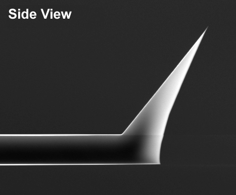
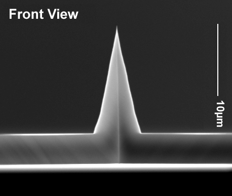
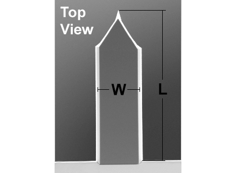
 Due to their unique geometry the tips of the AdvancedTEC probes are more susceptible to tip damage by electrostatic discharge (ESD) than other Silicon-SPM-Probes.