Rivera-Adorno FA, Sharpe SA, Olayemi TE, Ese JI, Fraund M, Moffet RC, TC A, Windwer E, Fang Z, Valencia-Acuña P, O’Callahan BT
Spectro-microscopic analysis of soot particle composition and source attribution
Aerosol Science and Technology. 2025 Jun 12:1-7
DOI: https://doi.org/10.1080/02786826.2025.2519101
Wang CF, Valencia-Acuna P, Krayev AV, El-Khoury PZ
Optical Extinction-Based 3D Nano-Imaging of WS2 on Gold
The Journal of Physical Chemistry Letters. 2024 Oct 3;15(40):10272-7.
DOI: https://doi.org/10.1021/acs.jpclett.4c02077
Fu X, Xu Y, Wang S, Lu H, Li J, Li Y, Su H, Liu S
NanoNeRF: Robot-assisted Nanoscale 360° reconstruction with neural radiance field under scanning electron microscope
In2024 IEEE/RSJ International Conference on Intelligent Robots and Systems (IROS) 2024 Oct 14 (pp. 1343-1348). IEEE
DOI: https://doi.org/10.1109/IROS58592.2024.10802598
Zhang H, Fu X, Liu S, Wang Y
Iterative Learning Embedded Composite Model Reference Adaptive Control for Off-Axis In-Situ Rotation in Nanorobotic Manipulation.
IEEE Control Systems Letters. 2023 Nov 24;8:291-6
DOI: https://doi.org/10.1109/LCSYS.2023.3336545
Geng J, Zhang H, Meng X, Gao H, Rong W, Xie H
Three-Dimensional Kelvin Probe Force Microscopy
ACS Applied Materials & Interfaces. 2022 Jul 11;14(28):32719-28
DOI: https://doi.org/10.1021/acsami.2c07645
Richheimer F, Vincent T, Catanzaro A, Huáng NJ, Baker MA, Dorey RA, Giusca CE, Castro FA, Kazakova O, Wood S
Probing nanoscale Schottky barrier characteristics at WSe2/graphene heterostructures via electrostatic doping
Advanced electronic materials. 2022 Sep;8(9):2200196
DOI: https://doi.org/10.1002/aelm.202200196
Rokni H, Lu W
Direct measurements of interfacial adhesion in 2D materials and van der Waals heterostructures in ambient air.
Nature Communications. 2020 Nov 5;11(1):5607
DOI: https://doi.org/10.1038/s41467-020-19411-7
Qu J, Liu X
Experimental investigation of the impact of SEM chamber conditions on the contact resistance of in-situ nanoprobing
In2017 International Conference on Manipulation, Automation and Robotics at Small Scales (MARSS) 2017 Jul 17 (pp. 1-6). IEEE
DOI: https://doi.org/10.1109/MARSS.2017.8001945
Kang K, Godin K, Kim YD, Fu S, Cha W, Hone J, Yang EH
Graphene‐Assisted Antioxidation of Tungsten Disulfide Monolayers: Substrate and Electric‐Field Effect
Advanced Materials. 2017 May;29(18):1603898.
DOI: https://doi.org/10.1002/adma.201603898
Qu J, Lee M, Hilke M, Liu X
Investigating the impact of SEM chamber conditions and imaging parameters on contact resistance of in situ nanoprobing
Nanotechnology. 2017 Jul 24;28(34):345702
DOI: https://doi.org/10.1088/1361-6528/aa79ea
Dunaevskiy M, Dontsov A, Alekseev P, Monakhov A, Baranov A, Girard P, Arinero R, Teissier R, Titkov A
Apertureless scanning microscope probe as a detector of semiconductor laser emission
Applied Physics Letters. 2015 Apr 27;106(17)
DOI: https://doi.org/10.1063/1.4919528
Alekseev PA, Dunaevskii MS, Slipchenko SO, Podoskin AA, Tarasov IY
Mapping of laser diode radiation intensity by atomic-force microscopy
Technical Physics Letters. 2015 Sep;41(9):870-3.
DOI: https://doi.org/10.1134/S1063785015090163
Xie H, Régnier S
Flexible Robotic AFM‐Based System for Manipulation and Characterization of Micro‐and Nano‐Objects
Micro‐and Nanomanipulation Tools. 2015 Nov 2:441-76
DOI: https://doi.org/10.1002/9783527690237.ch18
Acosta JC, Polesel-Maris J, Thoyer F, Xie H, Haliyo S, Régnier S
Gentle and fast atomic force microscopy with a piezoelectric scanning probe for nanorobotics applications
Nanotechnology. 2013 Jan 22;24(6):065502
DOI: https://doi.org/10.1088/0957-4484/24/6/065502
Machida S, Watanabe-Nakayama T, Saito M, Afrin R, Ikai A
Fabricated cantilever for AFM measurements and manipulations: pre-stress analysis of stress fibers.
Micron. 2012 Dec 1;43(12):1380-9
DOI: https://doi.org/10.1016/j.micron.2012.03.025
Xie H, Régnier S
3D Micro/nanomanipulation with force spectroscopy
InEncyclopedia of Nanotechnology 2012 (pp. 1-9). Springer, Dordrecht
DOI: https://doi.org/10.1007/978-90-481-9751-4_203
Chen Y, Hui X, Jihong Y, Jie Z
A New 3-D Assembly Approach For Nanoelectromechanical Switch Fabrication
In1st International Conference on Mechanical Engineering and Material Science (MEMS 2012) 2012 Dec (pp. 725-730). Atlantis Press
DOI: https://doi.org/10.2991/mems.2012.190


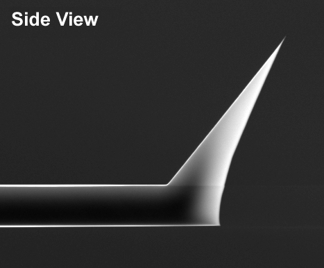
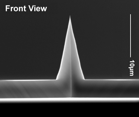
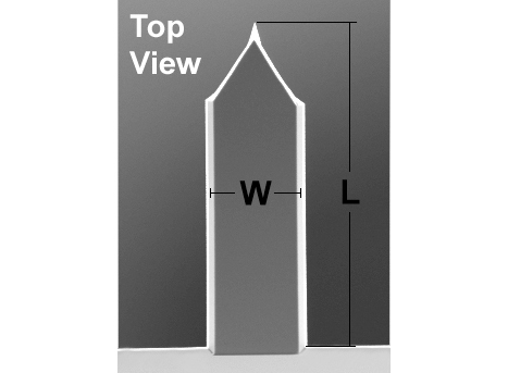
 Due to their unique geometry the tips of the AdvancedTEC probes are more susceptible to tip damage by electrostatic discharge (ESD) than other Silicon-SPM-Probes.