


Lateral-(XY)-Calibration Grating available from the NANOSENSORS™ Special Developments List
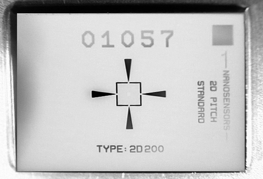
The grating (2D200) is used for a very precise x-y-calibration of the scanning mechanism. The grating consists of a 2-dimensional lattice of inverted square pyramids with 300nm pitch etched into a silicon chip.
Features:
- 200 nm pitch
- high accuracy
The silicon chip is glued onto a stainless steel sample holder with 12 mm diameter. This holder can be magnetically or mechanically fixed. The product will be shipped in a Gel-Pak® carrier.
This standard has been developed in close cooperation with the German national authority of standards: PTB (Physikalisch Technische Bundesanstalt). Due to this PTB is able to certify this standard in accordance with international guidelines. Please request further assistance from PTB working group 5.23 3D Nanometrologie directly - www.ptb.de.
Gel-Pak® is a registered trademark of Delphon Industries
Only available as long as supply lasts.
| Chip | |
|---|---|
| Chip size | 5 x 7 mm² |
| Active area | 100 x 100 µm² |
| The active area is located in the center of the chip and is surrounded by the FindMe structure. The lattice of inverted pyramids make up the active area. | |
| Lattice | |
| Pitch | 200 nm |
| Accuracy of pyramid position | 10nm |
| Accuracy of pitch (10x10 µm² scan) | 0.1% |
| Accuracy of pitch (100x100 µm² scan) | ±0.01% |
| Pyramids | |
| Edge length of square pyramids | approx. 50 nm |
| Sidewall angle (versus wafer surface) | 54.7° |
| Accuracy of sidewall angle | 0.5 |
| Depth of pyramids | approx. 70 nm |
| Order Code | Quantity | Data sheet |
|---|---|---|
| 2D200 | 1 | enclosed |